


- Description
- Reviews
- FAQs
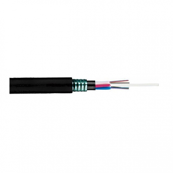
What Is QSFP+ 40G ER4 1310nm 40km Optical Transceiver Module RT-QSFP-40G-ER4
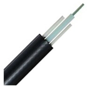
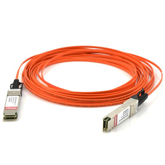
QSFP+ 40G ER4 1310nm 40km Optical Transceiver Module QSFP-40G-ER4 This product is a transceiver module designed for 2m-10km optical communication applications. The design is compliant to 40GBASE-LR4 of the IEEE P802.3ba standard. The module converts 4 inputs channels (ch) of 10Gb/s electrical data to 4 CWDM optical signals, and multiplexes them into a single channel for 40Gb/s optical transmission. Reversely, on the receiver side, the module optically de-multiplexes a 40Gb/s input into 4 CWDM channels signals, and converts them to 4 channel output electrical data.The central wavelengths of the 4 CWDM channels are 1271, 1291, 1311 and 1331 nm as members of the CWDM wavelength grid defined in ITU-T G.694.2. It contains a duplex LC connector for the optical interface and a 38-pin connector for the electrical interface. To minimize the optical dispersion in the long-haul system, single-mode fiber (SMF) has to be applied in this module.
Product Features
· Compliant with 40G Ethernet IEEE802.3ba and 40GBASE-LR4 Standard
· QSFP+ MSA compliant
· Compliant with QDR/DDR Infiniband data rates
· Up to 11.2Gb/s data rate per wavelength
· 4 CWDM lanes MUX/DEMUX design
· Up to 40km transmission on single mode fiber (SMF)
· Operating case temperature: 0 to 70℃
· Maximum power consumption 2.5W
· LC duplex connector
· RoHS compliant
Applications
· 40GBASE-ER4 Ethernet Links
· Infiniband QDR and DDR interconnects
· Client-side 40G Telecom connections
Absolute Maximum Ratings
It has to be noted that the operation in excess of any individual absolute maximum ratings might cause permanent damage to this module.
| Parameter | Symbol | Min | Max | Unit | Notes |
| Storage Temperature | TS | -40 | 85 | ℃ | |
| Operating Case Temperature | TOP | 0 | 70 | ℃ | |
| Power Supply Voltage | VCC | -0.5 | 3.6 | V | |
| Relative Humidity (non-condensation) | RH | 0 | 85 | % | |
| Damage Threshold, each Lane | THd | 3.3 | dBm |
Recommended Operating Conditions and Power Supply Requirements
| Parameter | Symbol | Min | Typical | Max | Unit | Notes |
| Operating Case Temperature | TOP | 0 | 70 | ℃ | ||
| Power Supply Voltage | VCC | 3.135 | 3.3 | 3.465 | V | |
| Data Rate, each Lane | 10.3125 | Gb/s | ||||
| Control Input Voltage High | 2 | VCC | V | |||
| Control Input Voltage Low | 0 | 0.8 | V | |||
| Link Distance with G.652 | D | 0.002 | 40 | km |
Electrical Characteristics
The following electrical characteristics are defined over the Recommended Operating Environment unless otherwise specified.
| Parameter | Test Point | Min | Typical | Max | Unit | Notes |
| Power Consumption | 2.5 | W | ||||
| Supply Current | ICC | 0.7 | A | |||
| Transceiver Power-on Initialization Time | 2000 | ms | 1 | |||
| Transmitter (each Lane) | ||||||
| Single-ended Input Voltage Tolerance (Note 2) | -0.3 | 4.0 | V | Referred to TP1 signal common | ||
| AC Common Mode Input Voltage Tolerance | 15 | mV | RMS | |||
| Differential Input Voltage Swing Threshold | 50 | mVpp | LOSA Threshold | |||
| Differential Input Voltage Swing | Vin,pp | 190 | 700 | mVpp | ||
| Differential Input Impedance | Zin | 90 | 100 | 110 | ohm | |
| Differential Input Return Loss | See IEEE 802.3ba 86A.4.11 | dB | 10MHz- 11.1GHz | |||
| J2 Jitter Tolerance | Jt2 | 0.17 | UI | |||
| J9 Jitter Tolerance | Jt9 | 0.29 | UI | |||
| Data Dependent Pulse Width Shrinkage (DDPWS ) Tolerance | 0.07 | UI | ||||
| Eye Mask Coordinates {X1, X2, Y1, Y2} | 0.11, 0.31 95, 350 | UI mV | Hit Ratio = 5×10⁻⁵ | |||
| Receiver (each Lane) | ||||||
| Single-ended Output Voltage | -0.3 | 4.0 | V | Referred to signal common | ||
| AC Common Mode Output Voltage | 7.5 | mV | RMS | |||
| Differential Output Voltage Swing | Vout,pp | 300 | 850 | mVpp | ||
| Differential Output Impedance | Zout | 90 | 100 | 110 | ohm | |
| Termination Mismatch at 1MHz | 5 | % | ||||
| Differential Output Return Loss | See IEEE 802.3ba 86A.4.2.1 | dB | 10MHz- 11.1GHz | |||
| Common Mode Output Return Loss | See IEEE 802.3ba 86A.4.2.2 | dB | 10MHz- 11.1GHz | |||
| Output Transition Time | 28 | Ps | 20% to 80% | |||
| J2 Jitter Output | Jo2 | 0.42 | UI | |||
| J9 Jitter Output | Jo9 | 0.65 | UI | |||
| Eye Mask Coordinates {X1, X2, Y1, Y2} | 0.29, 0.5, 150, 425 | UI mV | Hit Ratio = 5×10⁻⁵ | |||
Notes:
1. Power-on Initialization Time is the time from when the power supply voltages reach and remain above the minimum recommended operating supply voltages to the time when the module is fully functional.
2. The single ended input voltage tolerance is the allowable range of the instantaneous input signals.
Optical Characteristics
| Parameter | Symbol | Min | Typical | Max | Unit | Notes | |
| Wavelength Assignment | L0 | 1264.5 | 1271 | 1277.5 | nm | ||
| L1 | 1284.5 | 1291 | 1297.5 | nm | |||
| L2 | 1304.5 | 1311 | 1317.5 | nm | |||
| L3 | 1324.5 | 1331 | 1337.5 | nm | |||
| Transmitter | |||||||
| Side Mode Suppression Ratio | SMSR | 30 | dB | ||||
| Total Average Launch Power | PT | 8.3 | dBm | ||||
| Average Launch Power, each Lane | PAVG | -4 | 2.3 | dBm | |||
| Optical Modulation Amplitude (OMA), each Lane | POMA | -4 | 3.5 | dBm | 1 | ||
| Difference in Launch Power between any Two Lanes (OMA) | Ptx,diff | 6.5 | dB | ||||
| Launch Power in OMA minus Transmitter and Dispersion Penalty (TDP), each Lane | -4.8 | dBm | |||||
| TDP, each Lane | TDP | 2.6 | dB | ||||
| Extinction Ratio | ER | 3.5 | dB | ||||
| Relative Intensity Noise | RIN | -128 | dB/Hz | 12dB reflection | |||
| Optical Return Loss Tolerance | TOL | 20 | dB | ||||
| Transmitter Reflectance | RT | -12 | dB | ||||
| Transmitter Eye Mask Definition {X1, X2, X3, Y1, Y2, Y3} | {0.25, 0.4, 0.45, 0.25, 0.28, 0.4} | ||||||
| Average Launch Power OFF Transmitter, each Lane | Poff | -30 | dBm | ||||
| Receiver | |||||||
| Damage Threshold, each Lane | THd | 3.3 | dBm | 2 | |||
| Total Average Receive Power | 8.3 | dBm | |||||
| Average Receive Power, each Lane | -13.7 | 2.3 | dBm | ||||
| Receiver Reflectance | RR | -26 | dB | ||||
| Receiver Sensitivity (OMA), each Lane | SEN | -11.5 | dBm | ||||
| Stressed Receiver Sensitivity (OMA), each Lane | -9.6 | dBm | 3 | ||||
| Difference in Receive Power between any Two Lanes (OMA) | Prx,diff | 7.5 | dB | ||||
| LOS Assert | LOSA | -28 | dBm | ||||
| LOS Deassert | LOSD | -15 | dBm | ||||
| LOS Hysteresis | LOSH | 0.5 | dB | ||||
| Receiver Electrical 3 dB upper Cutoff Frequency, each Lane | FC | 12.3 | GHz | ||||
| Conditions of Stress Receiver Sensitivity Test (Note 5) | |||||||
| Vertical Eye Closure Penalty, each Lane | 1.9 | dB | |||||
| Stressed Eye J2 Jitter, each Lane | 0.3 | UI | |||||
| Stressed Eye J9 Jitter, each Lane | 0.47 | UI | |||||
Notes:
1. Even if the TDP < 0.8 dB, the OMA min must exceed the minimum value specified here.
2. The receiver shall be able to tolerate, without damage, continuous exposure to a modulated optical input signal having this power level on one lane. The receiver does not have to operate correctly at this input power.
3. Measured with conformance test signal at receiver input for BER = 1×10-12.
4. MVertical eye closure penalty and stressed eye jitter are test conditions for measuring stressed receiver sensitivity. They are not characteristics of the receiver.
Digital Diagnostic Functions
The following digital diagnostic characteristics are defined over the normal operating conditions unless otherwise specified.
| Parameter | Symbol | Min | Max | Unit | Notes |
| Temperature monitor absolute error | DMI_Temp | -3 | +3 | ℃ | Over operating temperature range |
| Supply voltage monitor absolute error | DMI_VCC | -0.1 | +0.1 | V | Over full operating range |
| Channel RX power monitor absolute error | DMI_RX_Ch | -2 | +2 | dB | 1 |
| Channel Bias current monitor | DMI_Ibias_Ch | -10% | +10% | mA | |
| Channel TX power monitor absolute error | DMI_TX_Ch | -2 | +2 | dB | 1 |
Notes:
1. Due to measurement accuracy of different single mode fibers, there could be an additional +/-1 dB fluctuation, or a +/- 3 dB total accuracy.
- Customers Reviews
-
 (0)
(0) (0)
(0) (0)
(0) (0)
(0) (0)
(0)
* Delivery Time.
We need 1-2 days to process your order before shipping. There are two shipping methoed.
Fast Delivery: The delivery time for US, European countries the delivery will take 3-5 days.
Slow Delivery: The delivery time for US, European countries the delivery will take 7-15 days.
* Tracking information.
After we ship package, customer receive automatic email with tracking details.
* Lost Package Policy.
If a package did not arrive in 2 weeks after the shipping date, then this package is treated as Lost. In this case a new package will be shipped to the customer provided we are able to give the same items as those purchased by the customer. If we are not able to provide the same items to substitute the lost ones we will either propose to the customer similar items or refund their cost as it will be mutually agree with the customer. If one or more items neither the same nor similar are available to be shipped, the customer can request to cancel the order entirely, thus the total cost of the order including shipping and handling cost will be fully refunded.


